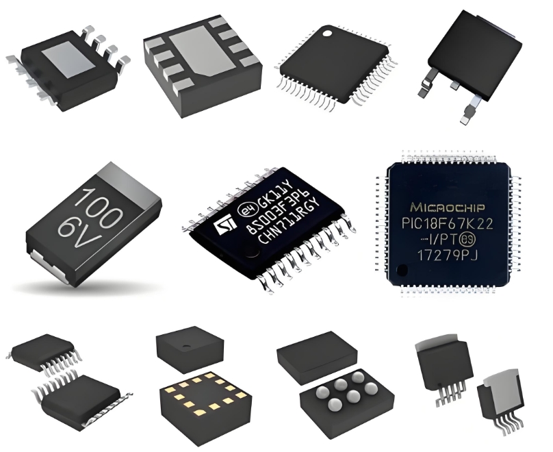
EEPROM Memory: Interfacing and Programming the Microchip 24LC64-I/ST Serial EEPROM Chip
Electrically Erasable Programmable Read-Only Memory (EEPROM) is a non-volatile memory technology crucial for storing small but critical data that must be retained when system power is removed. Parameters like calibration constants, device settings, and historical data are typical use cases. Among the various solutions available, the Microchip 24LC64-I/ST stands out as a popular and versatile 64 Kbit serial EEPROM chip. This article explores its key features and details the process of interfacing and programming it with a microcontroller.
The 24LC64 belongs to the 24XX series of I²C-compatible serial EEPROMs. The I²C (Inter-Integrated Circuit) protocol is a cornerstone of its design, requiring only two bidirectional open-drain lines for communication: a Serial Data Line (SDA) and a Serial Clock Line (SCL). This drastically reduces the number of I/O pins required on a microcontroller, making it ideal for space-constrained designs. The 24LC64 offers a memory array of 8192 x 8 (64 Kbit) and supports byte-level and page-level write operations, with a 64-byte page write buffer. This allows for efficient writing of multiple consecutive bytes in a single operation, speeding up data transfer.
A critical feature of this EEPROM is its built-in data protection. The memory array is divided into two blocks with a dedicated hardware write-protect (WP) pin. When the WP pin is tied to VCC, the upper quarter of the memory (1800h-1FFFh) is locked against write operations. When tied to GND, the entire memory is writable. This provides a robust method to prevent accidental data corruption for critical parameters.
Interfacing the 24LC64 with a Microcontroller
The hardware interface is remarkably simple. The SDA and SCL lines must be connected to the corresponding pins on the microcontroller, each requiring a pull-up resistor to VCC (typically 4.7 kΩ). The address pins (A0, A1, A2) are used to set the least significant bits of the 7-bit I²C device address, allowing up to eight 24LC64 devices to be connected on the same bus. The device address is formatted as 1010A2A1A0, where the user-defined bits (A2, A1, A0) are set by tying these pins to VCC or GND. The WP pin is connected to a microcontroller GPIO or directly to VCC/GND based on the required protection level.
Programming and Communication Protocol
Programming the chip involves executing standard I²C sequences. All communication is initiated by the microcontroller (Master) through a START condition and concluded with a STOP condition.
1. Byte Write: To write a single byte, the Master sends:
START bit.
Device address with R/W bit set to '0' (Write).
Most significant byte (MSB) of the memory address to write to.
Least significant byte (LSB) of the memory address.
The data byte to be stored.

STOP bit. The EEPROM then internally initiates the non-volatile write cycle (tWR), which typically takes 5 ms to complete. During this time, the chip will not acknowledge its address (a process known as polling).
2. Page Write: A page write is similar but allows up to 64 bytes to be written after the memory address is sent. The internal address pointer automatically increments after each data byte is received, wrapping around to the start of the page if the end is reached.
3. Sequential Read: To read data sequentially, the Master must first set the address pointer by performing a dummy write operation. It sends:
START, device address (Write), memory address (MSB, LSB).
Then, it sends a Repeated START condition.
It re-sends the device address with the R/W bit set to '1' (Read).
The EEPROM then begins transmitting data bytes. After each byte, the Master sends an Acknowledge. To stop reading, the Master responds with a Not Acknowledge (NACK) followed by a STOP condition.
A vital consideration for reliable operation is write-cycle timing. The microcontroller must observe the 5 ms write cycle time after initiating a write command. The most efficient method is to poll the device: after the STOP condition is sent for a write, the Master can repeatedly send a START followed by the device address (Write) until the chip responds with an Acknowledge, indicating the internal cycle is complete and it is ready for new commands.
ICGOODFIND: The Microchip 24LC64-I/ST is an exceptionally efficient and reliable solution for non-volatile data storage. Its simple two-wire I²C interface minimizes MCU pin usage, while its hardware write-protection and robust communication protocol ensure data integrity. Mastering the timing of its internal write cycle is the key to successfully integrating this powerful memory chip into any embedded system design.
Keywords:
EEPROM
I²C Protocol
Microcontroller Interfacing
Non-volatile Memory
Data Storage
